Product Summary
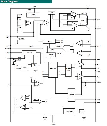
The SC488IMLTRT is a combination switching regulator and linear source/sink regulator intended for DDR1/2 memory systems. The purpose of the SC488IMLTRT is to generate the supply voltage, VDDQ, for the memory system. It is a pseudo-fixed frequency constant on-time controller designed for high efficiency, superior DC accuracy, and fast transient response. The purpose of the SC488IMLTRT is to generate the memory termination voltage, VTT, with the ability to source and sink 2.8A peak currents.
Parametrics
SC488IMLTRT absolute maximum ratings: (1)TON to VSSA: -0.3 to +25.0 V; (2)DH, BST to PGND1: -0.3 to +31.0 V; (3)BST, DH to LX: -0.3 to +6.0 V; (4)LX to PGND1: -2.0 to +25.0 V; (5)DL, ILIM, VDDP to PGND1: -0.3 to +6.0 V; (6)VDDP to DL: -0.3 to +6.0 V ; (7)VTTIN to PGND2; VTT to PGND2; VTTIN to VTT: -0.3 to +6.0 V; (8)EN/PSV, FB, PGD, REF, VCCA, VDDQS, VTTEN, VTTS to VSSA: -0.3 to +6.0 V; (9)VCCA to EN/PSV, FB, REF, VDDQS, VTT, VTTEN, VTTIN, VTTS: -0.3 to +6.0 V; (10)PGND1 to PGND2; PGND1 to VSSA; PGND2 to VSSA: -0.3 to +0.3V; (11)Thermal Resistance Junction to Ambient, θJA: 29℃/W; (12)Operating Junction Temperature Range TJ: -40 to +150℃; (13)Storage Temperature Range, TSTG: -65 to +150℃; (14)Peak IR Reflow Temperature, 10s - 40s TPKG: 260℃; (15)ESD Protection Level, VESD: 2kV.
Features
SC488IMLTRT features: (1)Constant On-Time Controller for Fast Dynamic Response on VDDQ; (2)DDR1/DDR2/DDR3 Compatible; (3)VDDQ = Fixed 1.8V or 2.5V, or Adjustable From 1.5V to 3.0V; (4)1.5% Internal Reference (2.5% System Accuracy); (5)Resistor Programmable On-Time for VDDQ; (6)VCCA/VDDP Range = 4.5V to 5.5V; (7)VIN Range = 2.5V to 25V; (8)Cycle-by-Cycle Current Limit for VDDQ; (9)Digital Soft-Start for VDDQ; (10)Analog Soft-Start for VTT/REF; (11)Smart Over-Voltage VDDQ Protection ; (12)Combined EN and PSAVE Pin for VDDQ; (13)Over-Voltage/Under-Voltage Fault Protection; (14)Power Good Output; (15)Separate VCCA and VDDP Supplies; (16)VTT/REF Range = 0.75V – 1.5V.
Diagrams

 |
 SC4808B-1 |
 Other |
 |
 Data Sheet |
 Negotiable |
|
||||
 (China (Mainland))


