(China (Mainland))

Product Summary
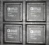
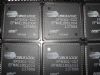
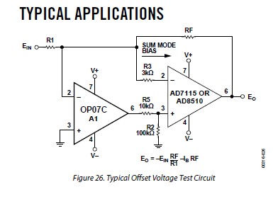
ADOP07 is the ultralow offset voltage operational amplifier which has very low input offset voltage (75 μV maximum for OP07E) that is obtained by trimming at the wafer stage. These low offset voltages generally eliminate any need for external nulling. The ADOP07 also features low input bias current (±4 nA for the OP07E) and high open-loop gain (200 V/mV for the OP07E). The low offset and high open-loop gain make the it particularly useful for high gain instrumentation applications.
Parametrics
ADOP07 absolute maximum ratings: (1)Supply Voltage (VS): ±22 V; (2)Input Voltage1: ±22 V; (3)Differential Input Voltage: ±30 V; (4)Storage Temperature Range S and P Packages: 65℃ to +125℃; (5)Operating Temperature Range: 0 to 70℃; (6)Junction Temperature: 150℃; (7)Lead Temperature, Soldering (60 sec): 300℃.
Features
ADOP07 features: (1)Low VOS: 75 μV maximum; (2)Low VOS drift: 1.3 μV/℃ maximum; (3)Ultrastable vs. time: 1.5 μV per month maximum; (4)Low noise: 0.6 μV p-p maximum; (5)Wide input voltage range: ±14 V typical; (6)Wide supply voltage range: 3 V to 18 V; (7)125℃ temperature-tested dice.
Diagrams
 |
 ADOP-27 |
Other |
|
Data Sheet |
Negotiable |
|
||||